Solar Energy Harvesting
Plasmonic Nanostructures
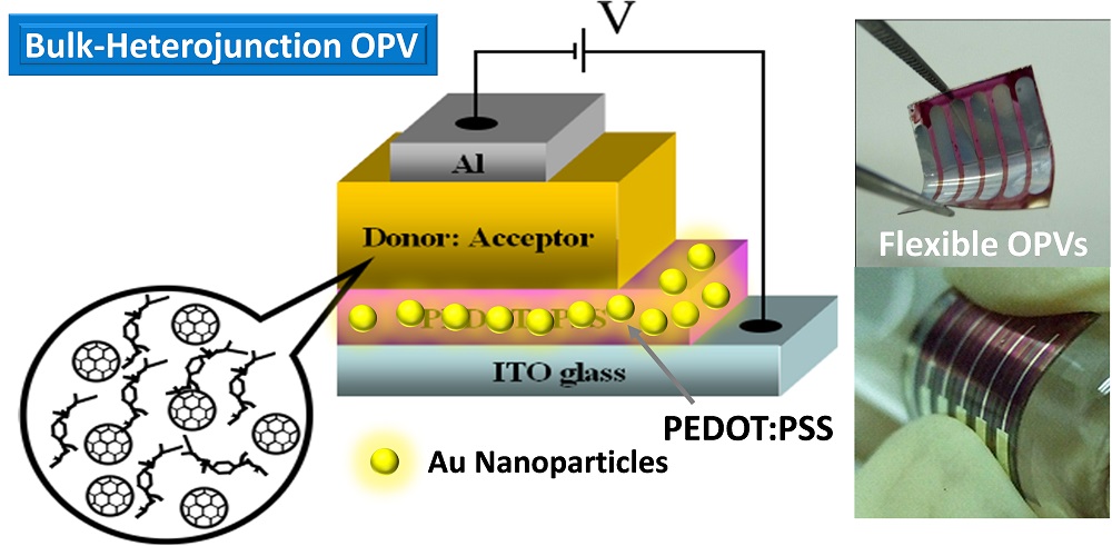
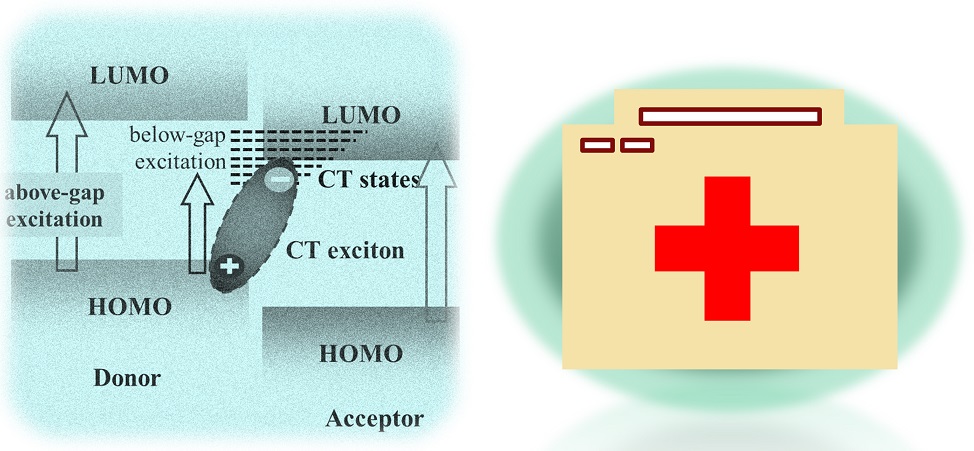
Surface plasmons (SPs) are associated with collective oscillations of free electrons at the metal surfaces. For metal nanoparticles (NPs), such as Au NPs, because the electrons are confined, the excited quanta is also called localized surface plasmon resonance (LSPR). Our group has investigated the effect of plasmonic nanostructures on the performance of polymer photovoltaic devices (OPVs) since 2009. We also synthesize novel nanoparticles, such as Au NP anchored on graphene oxides, and incorporate them into the OPVs for triggering the plasmonic effects. We also synthesis amphiphilic Au NPs so that they can be positioned into multiple locations in the OPVs. For details, please refer to our Review article.
Indoor Light Energy Harvesting
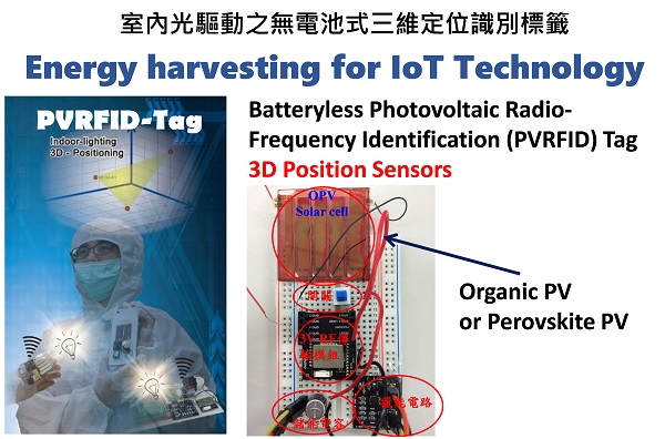
Many emerging photovoltaic drvices, incuding polymer photovoltaic devices (OPVs) and perovskite solar cells (PeSCs) exhibit very high power conversion efficiencies under low-level lighting conditions (Our Review Article). We, therefore, aim to develop photovoltaic devices, which are based on polymer and perovskite materials, for applications under low-level lighting conditions, such as indoor enviroment. For examples, we have demonstrated that tuning the enegy levels and band gaps is very critical for achieveing high performance (Read More). Plasmonic nanostructures can be also used to enhance the device power conversion efficiencies. To save energy and improve the sustainability of many electronic systems, such as Internet of Thing (IoT), OPVs and PeSCs could be ideal energy harvester from local enviroment. We have worked with Taiwan Semiconductor Research Institute, Prof. Chao, Prof. Liao and Prof. Chen in Department of Electrical and Computer Engineering (NCTU) to develop batteryless photovoltaic radio-frequency identification (PVRFID) tags. The primary fucntion of the tag is to indentify the location of the users. They could be very energy-efficient wireless position sensors in the future.
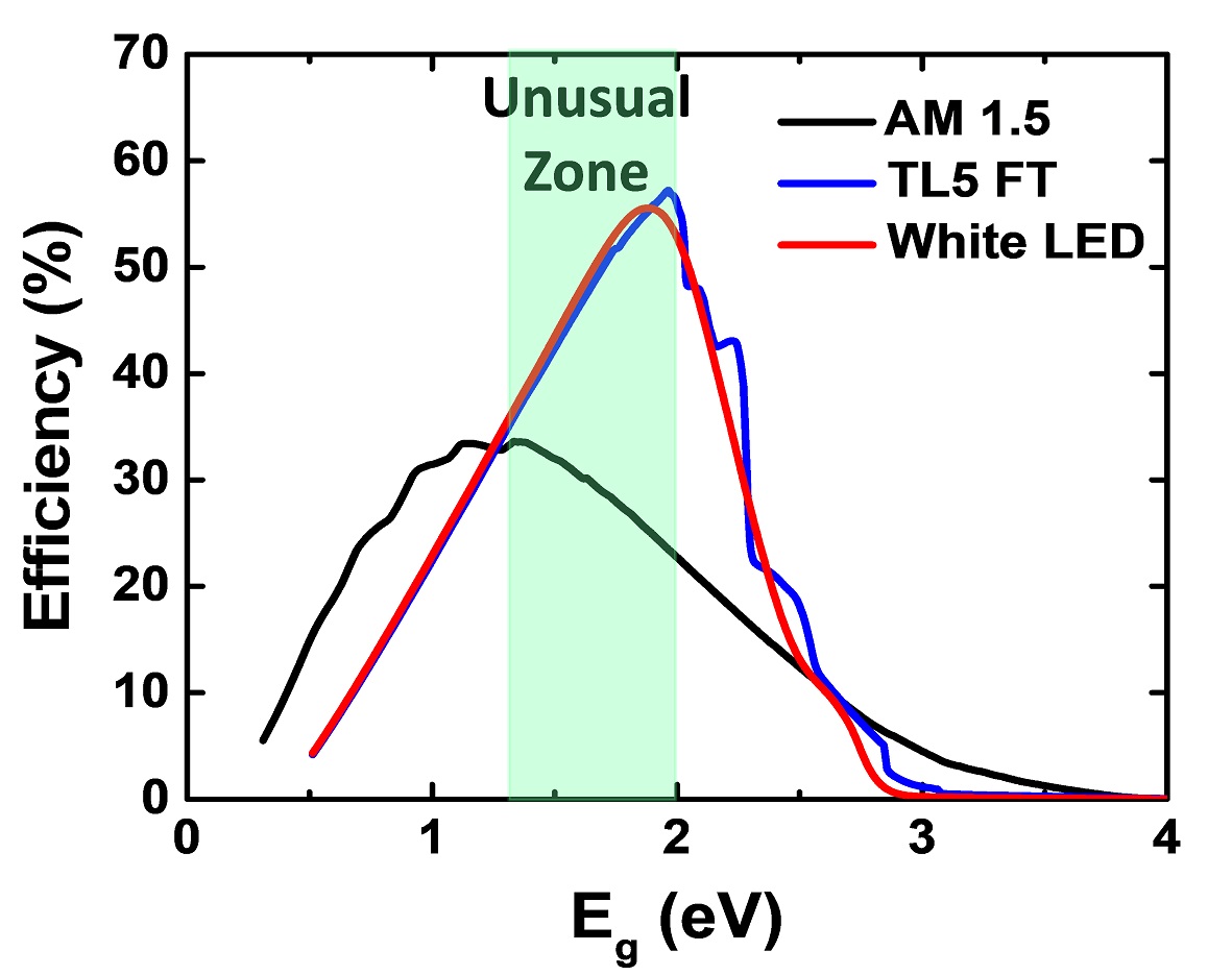
We recently calculate the Shockley‐Queisser limits under indoor light sources, including a fluorescent tube (FT) and a white LED (WLED); the results reveal an unusual bandgap (Eg) zone, in which the dependence of the power conversion efficiencies (PCEs) on the value of Eg exhibits different trends from that under solar irradiation. Accordingly, we tune the Eg of the perovskite films and the resulting perovksite photovoltaic devices featuring a wider band gap exhibited improved PCEs of 25.94 and 25.12% under illumination from an FT and a WLED, respectively. The experimental resluts validate our previous results of SQ limits (paper link).
Asymmetrical Perovskite Single Crystals
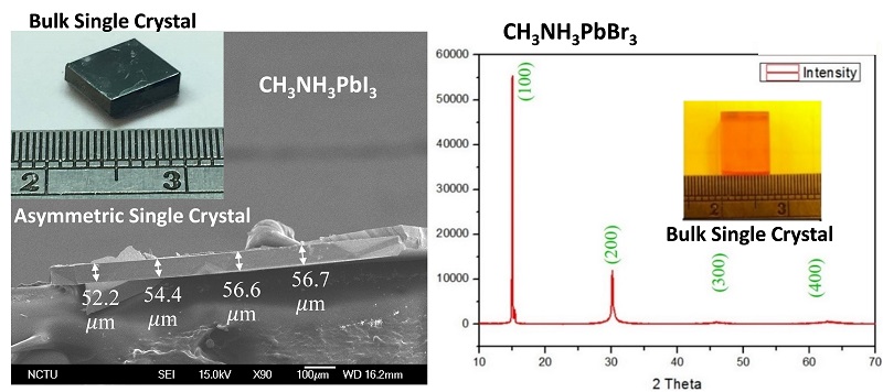
Perovksite single crystals (SCs) exhibit very long electron diffusion lengths and low defect density. In priciple, electronic devices made of single crystals should outperform the thin-film counterparts. However, many electronic applications require high-quality SCs in the form of thin films. Unfortunately, asymmetric perovskite SCs are very difficult to prepare using conventional thin film deposition techniques. We have developed a seeded space-limited inverse-temperature crystallization (SSLITC) for the successful growth of planar CH3NH3PbI3 SCs. Further, a PCE higher than 16% can be achieved using another novel space-limited crystallization method.
Flexible Waveguiding Photovoltaics
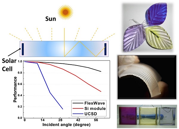
We have developed flexible solar concentrators for collecting sunlight economically and without sun trackers. Such device/module is called "Flexible Waveguiding Photovoltaics"(FWPVs). They are fabricated by integrating Si solar cells, a soft polydimethylsiloxane (PDMS) waveguide, and a TiO2-doped backside reflector. Further, after doping organic dyes in the PDMS waveguide, the segregated dyes induce strong scattering effects in the long-wavelength range, eventually leading to a record high optical efficiency for flexible luminescent solar concentrators. Based this technology, we spin off a start-up company, Flexwave.
Organic/Perovskite Light-Emitting Diodes
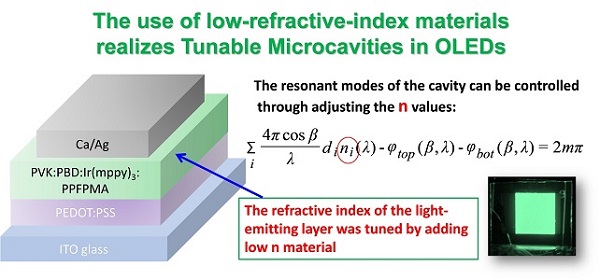
Prof. Chen started to study organic light-emitting diodes (OLEDs) since he was a PhD. student. He focused on the investigation of the properties and fabrication of triple (phosphorescent) OLEDs. We now still develop methods for improving the efficiencies of OLEDs. For example, through using microlense arrays and low refractive index polymers, we were able to improve the light out-coupling deficiencies. Currently, we are also very interested in developing high-performance perovskite light-emitting diodes and perovskite quantum dots.
Organic Thin-Film Transistors
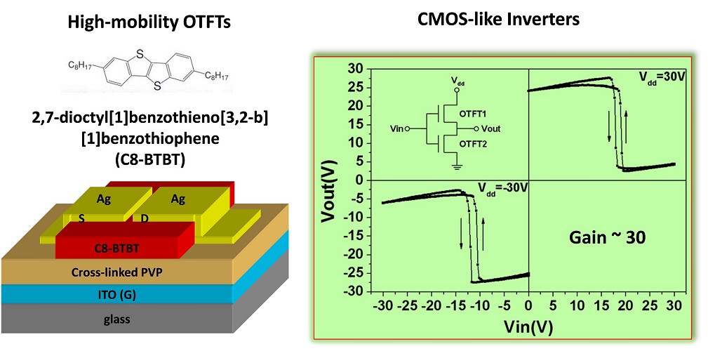
Organic thin-film transistions (OTFTs) are very useful for many applications, such as flat-panel displays and sensors. We also develop many methods for enhancing their performnace and functionalities. For examples, we have investigated the morphologic effects of the semiconductors on the device performance and develped high-k dielectric layers. We also fabricated transparent OTFTs, color-filtering functional OTFTs and various flexible OTFTs . By using a new fabrication scheme, our OTFTs have achieved a high mobility of 10 cm2V-1sec-1.
Machine Learning for Smart Materials
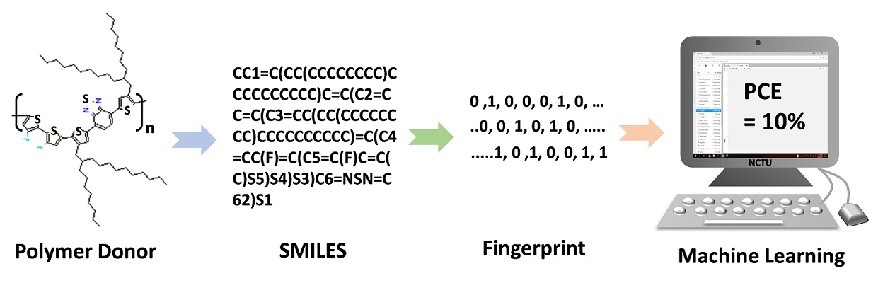
We have empolyed machine learning algorithms, such as random forest (RF) and support vector machine (SVM), for predicting the power conversion efficiencies (PCEs) of polymer solar cells from the chemical structures of the polymer donors in the devices. The PCEs of the device prepared with the polymer candidates can be predicted using their structure fingerprints as the only inputs. In other words, no preliminary material properties are required. We believe the results can help the virtual screening of organic semiconductors for solar applications, thereby accelerating design and synthesis of high-performance organic semiconductor materials using artificial intelligent.
Organic Photodetectors
We have fabricated organic photomultiple photodetectors, which means one photon can induce many electrons. They exhibit high sentivity, low operation voltage, and broadband response. The spectral response can be further extended to the near-infrared (NIR) region (1200 nm). These photodetectors can be used in fields of touch sensors, artificial eyeballs, and night vision.
Others